Logic Circuits
Finding 0-Hazards
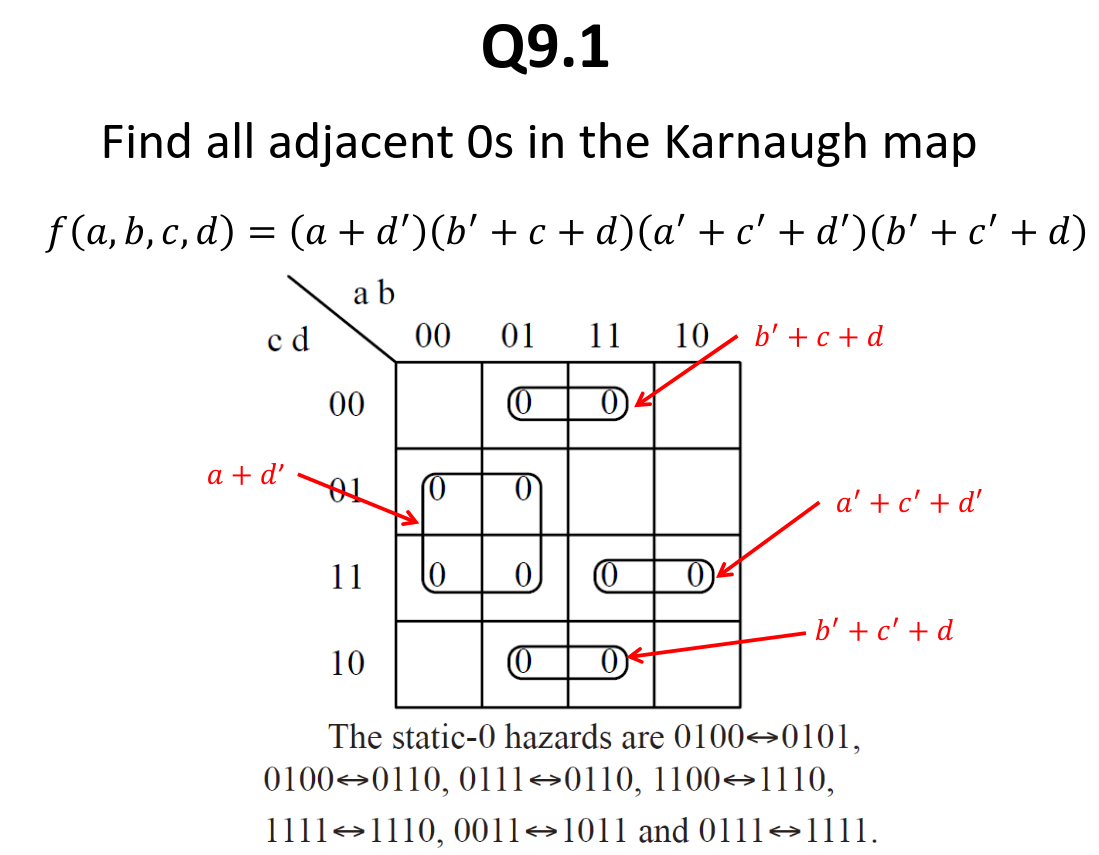
A two-level circuit implements the function \(f(a, b, c, d) = (a + d')(b' + c + d)(a' + c' + d')(b' + c' + d)\)
Q10.1 : How many 0-hazards are in the circuit?
Q10.2 : Redesign the circuit as a two-level circuit free of all hazards and using a minimum number of gates
Part 1: Understanding the Problem (Q10.1)
The Goal: Find the number of "Static-0 Hazards" in the circuit.
What is a Static-0 Hazard?
In a Product of Sums (POS) circuit (which groups 0s), the output should stay 0 when inputs change between adjacent cells that are both 0.
- However, if you move between two adjacent
0cells that represent different groups (terms) in your equation, and there is no single group covering both, the output might momentarily glitch to1. - This glitch is a Static-0 Hazard.
Step-by-Step Solution:
-
Map the Equation to the K-Map (Image Q9.1): The function is \(f = (a+d')(b'+c+d)(a'+c'+d')(b'+c'+d)\). We place a
0in the K-map for every condition that makes a term equal to 0.- \((a+d')\) creates the vertical group of four 0s on the left (Cells 1, 3, 5, 7).
- \((b'+c+d)\) creates the two 0s at indices 4 and 12.
- \((a'+c'+d')\) creates the two 0s at indices 11 and 15.
- \((b'+c'+d)\) creates the two 0s at indices 6 and 14.
-
Identify the Hazards: Look at the K-map in Q9.1. A hazard exists at any boundary between two
0s that are NOT encircled by the same black loop.Let's trace the arrows in the solution image: * Cell 4 (0100) \(\leftrightarrow\) Cell 5 (0101): Cell 4 is in the \((b'+c+d)\) group. Cell 5 is in the \((a+d')\) group. No shared loop. (Hazard 1) * Cell 4 (0100) \(\leftrightarrow\) Cell 12 (1100): These are in the same loop group from the original equation? No, looking at the diagram, the groups are separate pairs. Wait, 4 and 12 are vertically adjacent. If the original equation groups them differently, it's a hazard. The diagram shows them as separate groups. (Hazard) * Cell 7 (0111) \(\leftrightarrow\) Cell 6 (0110): Cell 7 is in the left strip. Cell 6 is in the separate bottom strip. No shared loop. (Hazard) * Cell 15 (1111) \(\leftrightarrow\) Cell 14 (1110): Different groups. (Hazard)
Basically, find every instance where two 0s touch, but the black loops drawn in Q9.1 do not overlap across that boundary.
The Answer: The list at the bottom of Q9.1 enumerates exactly which transitions cause these glitches (e.g., \(0100 \leftrightarrow 0101\)).
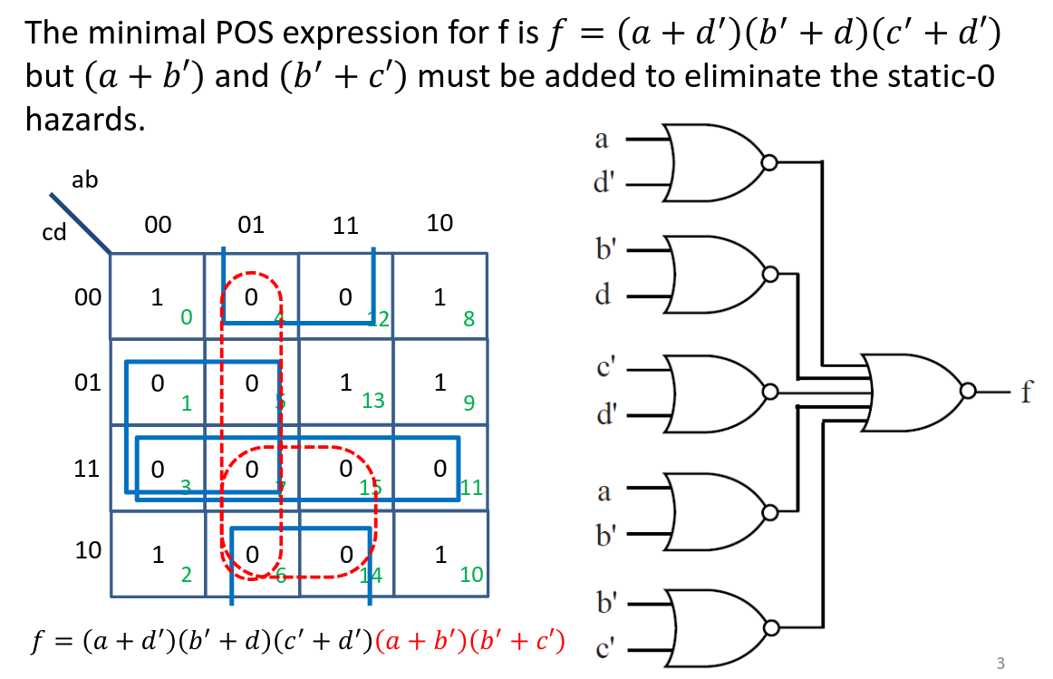
Part 2: Designing a Hazard-Free Circuit (Q10.2)
The Goal: Redesign the circuit to remove these hazards using the minimum number of gates.
How to Fix Hazards: To eliminate a hazard between two adjacent groups, you must add a redundant term (a new loop) that covers both adjacent cells. This is often called a "consensus term."
Step-by-Step Solution (Image Q9.2):
-
Simplify the Base Logic (Blue Lines): First, find the Minimal POS expression (the simplest standard equation). Look at the Solid Blue Boxes in Q9.2.
- Group 1 (Left Column): Covers cells 1, 3, 5, 7. Expression: \((a + d')\).
- Group 2 (Right Vertical Strip): Covers cells 3, 7, 11, 15. Expression: \((c' + d')\).
- Group 3 (Horizontal Rect): Covers cells 4, 6, 12, 14. Expression: \((b' + d)\).
- Base Equation: \(f = (a+d')(b'+d)(c'+d')\).
-
Add Hazard Covers (Red Dashed Lines): Now, look for adjacent 0s from the Blue groups that are not covered by a single group.
- Problem: The Blue Group 1 (cells 5, 7) touches Blue Group 3 (cells 4, 6).
- Fix: Add a loop that covers all of them (4, 5, 6, 7). This is the Red Dashed Box in the middle.
-
Term: This grouping corresponds to \((a + b')\).
-
Problem: The Blue Group 3 (cells 6, 14) touches Blue Group 2 (cells 7, 15).
- Fix: Add a loop that covers overlapping area (6, 7, 14, 15). This is the Red Dashed Box on the bottom right.
- Term: This grouping corresponds to \((b' + c')\).
-
Final Equation: Combine the minimal terms (Blue) and the hazard-protection terms (Red): $\(f = \underbrace{(a+d')(b'+d)(c'+d')}_{\text{Minimal Logic}} \underbrace{(a+b')(b'+c')}_{\text{Hazard Protection}}\)$
-
Draw the Circuit: The circuit diagram on the right of Q9.2 implements this final equation.
- Inputs go into OR gates (represented by the curved shapes on the left).
- The outputs of those OR gates go into a single AND gate (represented by the shape on the right).
- Note on symbol drawing: The diagram uses NOR-NOR logic symbols (OR with inverted output feeding into an AND with inverted inputs), which is functionally equivalent to the OR-AND structure required for a POS expression.
Summary
- Q10.1 Answer: You count hazards by finding adjacent 0s on the K-map that don't belong to the same circled group.
- Q10.2 Answer: You fix the circuit by simplifying the groups first, then adding extra "overlapping" loops (red dashed lines) anywhere two groups touch. This ensures that when the input changes, the output is "held" at 0 by the overlapping group, preventing the glitch.
Solving two K-Maps
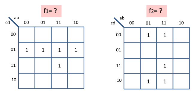
Obtain f₁ and f₂ for the 2-output circuit represented above and compare #gates and #gate inputs. Q9.1: Obtain minimum SOP of f₁ and f₂ individually Q9.2: Obtain a more economical solution.
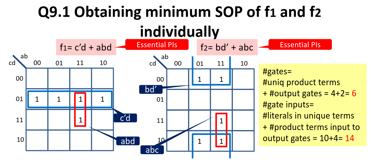
Part 1: Solving for \(f_1\) (Left Map)
Goal: Group the 1s into the largest possible groups of powers of 2 (1, 2, 4, 8...) to simplify the expression.
-
Identify the 1s:
- There is a row of four 1s at row
01. - There is a single 1 at row
11, column11.
- There is a row of four 1s at row
-
Group 1 (The Blue Rectangle):
- We can group the entire second row (row
01). - Analysis:
- Rows: The group stays entirely in row
01(\(c=0, d=1\)). Since \(c\) is 0, we write \(c'\). Since \(d\) is 1, we write \(d\). - Columns: The group spans all columns (00, 01, 11, 10). Because \(a\) and \(b\) change values throughout this group (0 to 1), they are eliminated.
- Rows: The group stays entirely in row
- Term: \(c'd\)
- We can group the entire second row (row
-
Group 2 (The Red Rectangle):
- We need to cover the remaining 1 at position
11, 11(bottom right of the populated area). - K-Map rules allow us to overlap groups. We group this 1 with the one directly above it (at
01, 11) to make a vertical pair. - Analysis:
- Columns: Both are in column
11(\(a=1, b=1\)). So, we keep \(ab\). - Rows: It covers row
01(\(d=1\)) and row11(\(d=1\)). The variable \(c\) changes (0 to 1), so it is eliminated. The variable \(d\) stays 1.
- Columns: Both are in column
- Term: \(abd\)
- We need to cover the remaining 1 at position
Final Expression for \(f_1\): $\(f_1 = c'd + abd\)$
Part 2: Solving for \(f_2\) (Right Map)
Goal: Cover the specific pattern of 1s in the second map.
-
Identify the 1s:
- Row
00: Columns01and11. - Row
11: Column11. - Row
10: Columns01and11.
- Row
-
Group 1 (The Blue Square):
- Look at the four 1s in the "corners" of the active area (Row 00 and Row 10).
- We can group the two 1s in the top row (Row 00) with the two 1s in the bottom row (Row 10). In K-maps, the top and bottom edges wrap around and are adjacent.
- Analysis:
- Rows: Row
00(\(d=0\)) and Row10(\(d=0\)). The variable \(c\) changes, but \(d\) remains 0 (\(d'\)). - Columns: Columns
01(\(b=1\)) and11(\(b=1\)). The variable \(a\) changes, but \(b\) remains 1 (\(b\)).
- Rows: Row
- Term: \(bd'\)
-
Group 2 (The Red Rectangle):
- We still need to cover the 1 at
11, 11. - We group it with the 1 directly below it* at
10, 11. - Analysis:
- Columns: Both are in column
11(\(a=1, b=1\)). So, we keep \(ab\). - Rows: Row
11(\(c=1\)) and Row10(\(c=1\)). The variable \(c\) remains 1. The variable \(d\) changes.
- Columns: Both are in column
- Term: \(abc\)
(Note: In the provided image, the red box looks like it spans a gap, but logically it is grouping the cell at Row 11/Col 11 with the cell at Row 10/Col 11. These are adjacent rows in the map).
- We still need to cover the 1 at
Final Expression for \(f_2\): $\(f_2 = bd' + abc\)$
Part 3: Calculating Costs (#Gates and #Inputs)
The problem asks for the cost of the individual implementation (meaning we build two separate circuits, one for \(f_1\) and one for \(f_2\), without sharing logic between them).
1. Counting Gates
We assume a standard 2-level implementation: AND gates to create the terms, and OR gates to combine them.
- For \(f_1\) (\(c'd + abd\)):
- 1 AND gate for \(c'd\)
- 1 AND gate for \(abd\)
- 1 OR gate to sum them.
- Total: 3 Gates.
- For \(f_2\) (\(bd' + abc\)):
- 1 AND gate for \(bd'\)
- 1 AND gate for \(abc\)
- 1 OR gate to sum them.
- Total: 3 Gates.
Total Gates = 3 + 3 = 6 Gates.
2. Counting Gate Inputs
The slide uses the formula:
#literals in unique terms + #product terms input to output gates
A. Literals (Inputs to the AND gates): Count the number of letters in each term.
- \(c'd\): 2 literals (inputs)
- \(abd\): 3 literals (inputs)
- \(bd'\): 2 literals (inputs)
- \(abc\): 3 literals (inputs)
- Sum: \(2 + 3 + 2 + 3 = \mathbf{10}\)
B. Inputs to Output Gates (Inputs to the OR gates): Count how many wires go into the OR gates.
- The \(f_1\) OR gate takes 2 wires (from the two AND gates).
- The \(f_2\) OR gate takes 2 wires (from the two AND gates).
- Sum: \(2 + 2 = \mathbf{4}\)
Total Gate Inputs = 10 (literals) + 4 (OR inputs) = 14 Inputs.
True or False Questions
1. A NOT gate is used to generate the complement of an input signal. Answer: \(\bigcirc\) (Correct)
- Reason: This is the definition of a NOT gate (inverter); if the input is 1, the output is 0, and vice versa.
2. In a combinational circuit, a static 1-hazard occurs when the output temporarily changes to 0, even though it should remain at 1. Answer: \(\bigcirc\) (Correct)
- Reason: A static 1-hazard is exactly defined as a momentary glitch to logic 0 when the output is supposed to hold a steady logic 1.
3. The difference between a flip-flop and a latch is that a flip-flop changes state only on the clock edge. Answer: \(\bigcirc\) (Correct)
- Reason: Latches are level-sensitive (they change state as long as the enable signal is active), whereas flip-flops are edge-triggered (changing state only on the rising or falling edge of a clock).
4. A 4-bit shift register performing a normal right shift (padding 0 into the most significant bit) reduces the binary value of the stored data by half (assuming unsigned representation). Answer: \(\bigcirc\) (Correct)
- Reason: In binary arithmetic, shifting bits to the right by one position is equivalent to integer division by 2 (e.g., \(0100_2\) is 4, shifted right becomes \(0010_2\), which is 2).
5. A T flip-flop toggles its output state when the T input is 1. Answer: \(\bigcirc\) (Correct)
- Reason: The "T" stands for Toggle. When \(T=1\), the next state is the inverse of the current state ($Q' $). When \(T=0\), the state holds (\(Q\)).
6. A decoder with \(n\) input lines generates \(2^n\) outputs, corresponding to the minterms of the input variables. Answer: \(\bigcirc\) (Correct)
- Reason: A standard binary decoder takes \(n\) inputs and activates exactly one of \(2^n\) outputs, which corresponds to the specific minterm of the input combination.
7. A Johnson counter with \(n\) flip-flops cycles through \(2^n\) unique states. Answer: \(\times\) (Incorrect)
- Reason: A Johnson counter (or twisted ring counter) with \(n\) flip-flops has \(2n\) states, not \(2^n\). (A standard binary counter would have \(2^n\) states).
8. The characteristic equation of a D flip-flop is \(Q^* = D'Q + DQ'\). Answer: \(\times\) (Incorrect)
- Reason: The characteristic equation of a D flip-flop is simply \(Q^* = D\) (the next state equals the input). The equation given (\(D'Q + DQ'\)) describes an XOR operation, which is actually the characteristic equation for a T flip-flop (where \(T=D\)).
9. If the output of a logic circuit updates only on a specific rising clock edge, the circuit is classified as asynchronous. Answer: \(\times\) (Incorrect)
- Reason: Circuits that update based on a specific clock edge are classified as synchronous. Asynchronous circuits do not rely on a global clock signal for state changes.
10. For a 2-to-1 multiplexer, if the select signal is 0, the output is always low. Answer: \(\times\) (Incorrect)
- Reason: If the select signal is 0, the output connects to Input 0 (Data 0). The output will be whatever value is present at Input 0 (which could be high or low), not necessarily "always low."
Question 2
The following is a circuit that utilizes a multiplexer (MUX). Consider a circuit where two four-bit unsigned integers, \(A = a_3a_2a_1a_0\) and \(B = b_3b_2b_1b_0\), are input into the multiplexer. In this circuit, when \(c_4 = 1\), \(A > B\), and in this case, the output \(Z\) is \(A\). Conversely, when \(c_4 = 0\), \(A \le B\), and in this case, the output \(Z\) is \(B\). Also, set \(c_0 = 0\). Now, consider the logic expressions representing the outputs of circuits \(N_0\) to \(N_3\). Specifically, given that circuits \(N_0\) to \(N_3\) are identical, express the output \(c_{i+1}\) of circuit \(N_i\) in terms of \(c_i\), \(a_i\), and \(b_i\) in the minimum sum-of-products form. Provide intermediate steps using Karnaugh maps in your explanation.
After completing the above 4-bit unsigned comparison, extend your design to handle 5-bit signed integers by introducing sign bits \(a_4\) and \(b_4\). Based on the following given circuit, create a 5-bit signed comparator circuit.
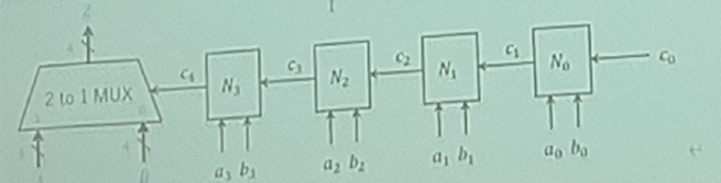
Part 1: Deriving the Logic for \(c_{i+1}\) (Unsigned Comparison)
Analysis: The circuit determines if \(A > B\). The signal \(c\) ripples from the Least Significant Bit (LSB) to the Most Significant Bit (MSB).
- \(c_4 = 1\) implies \(A > B\).
- \(c_4 = 0\) implies \(A \le B\).
- \(c_0 = 0\).
Let's define the meaning of the carry signal \(c_{i+1}\) at any stage \(i\):
- \(c_{i+1} = 1\) means the portion of \(A\) processed so far (\(a_i \dots a_0\)) is strictly greater than the portion of \(B\) (\(b_i \dots b_0\)).
- \(c_{i+1} = 0\) means the portion of \(A\) processed so far is less than or equal to \(B\).
Truth Table for Stage \(N_i\): Inputs: \(a_i, b_i\) (current bits), \(c_i\) (result from lower bits). Output: \(c_{i+1}\).
- If \(a_i > b_i\) (i.e., \(1, 0\)): Since bit \(i\) is more significant than bits \(0 \dots i-1\), \(A > B\) regardless of the lower bits. Result: 1.
- If \(a_i < b_i\) (i.e., \(0, 1\)): Similarly, \(A < B\) regardless of lower bits. Result: 0.
- If \(a_i = b_i\) (i.e., \(0, 0\) or \(1, 1\)): The current bits are equal, so the decision relies on the result from the lower bits (\(c_i\)). Result: \(c_i\).
| \(a_i\) | \(b_i\) | \(c_i\) | \(c_{i+1}\) | Minterm |
|---|---|---|---|---|
| 0 | 0 | 0 | 0 | |
| 0 | 0 | 1 | 1 | \(m_1\) |
| 0 | 1 | 0 | 0 | |
| 0 | 1 | 1 | 0 | |
| 1 | 0 | 0 | 1 | \(m_4\) |
| 1 | 0 | 1 | 1 | \(m_5\) |
| 1 | 1 | 0 | 0 | |
| 1 | 1 | 1 | 1 | \(m_7\) |
Karnaugh Map:
We map the minterms (1, 4, 5, 7) to a K-Map.
| \(a_ib_i\) \ \(c_i\) | 0 | 1 |
|---|---|---|
| 00 | 0 | 1 |
| 01 | 0 | 0 |
| 11 | 0 | 1 |
| 10 | 1 | 1 |
Grouping:
- Group 1 (Red): Pair in row 10 (\(m_4, m_5\)). Corresponds to \(a_i=1, b_i=0\). Term: \(a_i \overline{b_i}\).
- Group 2 (Green): Vertical pair in column 1 (\(m_5, m_7\)). Corresponds to \(a_i=1, c_i=1\). Term: \(a_i c_i\).
- Group 3 (Blue): Wrapping/Vertical pair in column 1 (\(m_1, m_5\)). Corresponds to \(b_i=0, c_i=1\). Term: \(\overline{b_i} c_i\).
Minimum Sum-of-Products Expression: $\(c_{i+1} = a_i \overline{b_i} + a_i c_i + \overline{b_i} c_i\)$
Part 2: 5-bit Signed Comparator Circuit
Logic Extension: For signed integers (2's complement), the Most Significant Bit (MSB) is the sign bit (\(a_4, b_4\)).
- \(0\) indicates Positive.
- \(1\) indicates Negative.
The logic for "greater than" reverses for the sign bit because a positive number (0) is mathematically greater than a negative number (1).
- If \(a_4=0\) (Pos) and \(b_4=1\) (Neg), then \(A > B\). (We want Output 1).
- If \(a_4=1\) (Neg) and \(b_4=0\) (Pos), then \(A < B\). (We want Output 0).
- If signs are equal (\(a_4=b_4\)), we treat the remaining magnitude bits normally (pass \(c_4\)).
Deriving the Sign Stage Logic (\(N_{sign}\)): We need an output \(Z\) based on inputs \(a_4, b_4, c_4\).
- Target behavior: \(Z = 1\) when \(A > B\).
- This yields the expression: \(Z = \overline{a_4} b_4 + \overline{a_4} c_4 + b_4 c_4\)
Comparison with \(N_i\):
- Standard \(N_i\) output: \(a \overline{b} + a c + \overline{b} c\)
- Signed \(N_{sign}\) output: \(\overline{a} b + \overline{a} c + b c\)
Notice that the Signed logic is identical to the Standard logic if we swap the inputs \(a\) and \(b\).
- If we feed \(b_4\) into the '\(a\)' input of an \(N\) block, and \(a_4\) into the '\(b\)' input, the block calculates: \(b_4 \overline{a_4} + b_4 c_4 + \overline{a_4} c_4\), which is exactly what we need.
Final Design:
- Take the existing chain \(N_0 \rightarrow N_1 \rightarrow N_2 \rightarrow N_3\).
- Add an identical block \(N_4\) to the left of \(N_3\).
- Connect the output of \(N_3\) (\(c_4\)) to the carry input (\(c\)) of \(N_4\).
- Important: Connect the sign bit \(b_4\) to the \(a\) input of \(N_4\), and \(a_4\) to the \(b\) input of \(N_4\).
- The output of \(N_4\) is the final control signal for the MUX (\(c_5\)).
Answer for the diagram:
Answer: \(c_{i+1} = a_i \overline{b_i} + a_i c_i + \overline{b_i} c_i\)
5-bit signed comparator circuit: (Draw a block \(N_4\) to the left of \(N_3\). Connect \(N_3\)'s output to \(N_4\)'s right input. Feed \(b_4\) into the pin labeled \(a_4\) and \(a_4\) into the pin labeled \(b_4\)).
Schematic representation:
           Z (Output)
           ^
      [ 2 to 1 MUX ]
      ^     ^      ^
      |     |      |
      A     B      | c_5 (final result)
                   |
            +------+
            |
      +-----+-----+      +-----------+           +-----------+
      |    N_4    |<-----|    N_3    |<-- ... <--|    N_0    |<-- c_0 (0)
      +--+-----+--+      +-----------+           +-----------+
         ^     ^
         |     |
         |     |
Input a: b_4   a_4
Input b: a_4   b_4
(Note: For block \(N_4\), the input labeled 'a' receives signal \(b_4\), and input 'b' receives signal \(a_4\). This effectively inverts the logic for the sign bit comparison.)
Question 3
Based on the image provided, here are the questions transcribed from the document:
Q3 Answer the following questions (a) to (e). In cases where inverted inputs are required as input to the circuit, always use inverted inputs (e.g., the inverted input of \(A\) is denoted as \(A'\)), and do not use inverters.
(a) Logic Expression and Circuit Diagram
Construct the logic expression \(F(A, B, C, D) = A'C + B'C' + CD\) using three two-input AND gates and one three-input OR gate, and draw the circuit diagram.
Logic Expression: The expression is given as: $\(F(A, B, C, D) = A'C + B'C' + CD\)$
Circuit Diagram Construction: To construct this using three two-input AND gates and one three-input OR gate:
- AND Gate 1: Inputs \(A'\) and \(C\). Output is \(A'C\).
- AND Gate 2: Inputs \(B'\) and \(C'\). Output is \(B'C'\).
- AND Gate 3: Inputs \(C\) and \(D\). Output is \(CD\).
- OR Gate: Takes the outputs of the three AND gates (\(A'C\), \(B'C'\), \(CD\)). Output is \(F\).
(Note: In the diagram, \(A', B', C'\) are supplied directly as inputs per the instructions.)
(b) NAND Circuit Construction
Construct the circuit from (a) using three two-input NAND gates and one three-input NAND gate, and draw the circuit diagram.
To convert the AND-OR circuit to a NAND-NAND circuit, we apply double inversion (\(F = F''\)) and De Morgan's laws. The structure remains similar, but gates are replaced with NANDs.
- Logic: \(F = ((A'C)' \cdot (B'C')' \cdot (CD)')'\)
- Components:
- Gate 1 (2-input NAND): Inputs \(A', C\). Output \(=(A'C)'\).
- Gate 2 (2-input NAND): Inputs \(B', C'\). Output \(=(B'C')'\).
- Gate 3 (2-input NAND): Inputs \(C, D\). Output \(=(CD)'\).
- Gate 4 (3-input NAND): Inputs are the outputs of Gates 1, 2, and 3. Output \(= F\).
(c) Static 1-Hazard Analysis
In the circuit from (b), a static 1-hazard occurs. List all the "input signal transition patterns" in which a static 1-hazard occurs. Also, explain the reason for the hazard using a Karnaugh map. Note that the explanation must include the terms "gate delay" and "input to the NAND gate in the output stage of F".
Input Signal Transition Patterns: A static 1-hazard occurs when the circuit output should remain at logic 1 during an input transition but momentarily glitches to 0. This happens when the transition crosses the boundary between two adjacent groupings (prime implicants) in the Karnaugh map that are not covered by a common redundant term.
In this circuit, the hazard occurs when switching between the term \(B'C'\) (where \(C=0\)) and the terms \(A'C\) or \(CD\) (where \(C=1\)). Specifically, when inputs \(A=0, B=0\) are held constant and \(C\) changes.
- Transition Pattern 1: \((A, B, D) = (0, 0, 0)\) while \(C\) changes \(0 \leftrightarrow 1\). (Binary \(0000 \leftrightarrow 0010\)).
- Transition Pattern 2: \((A, B, D) = (0, 0, 1)\) while \(C\) changes \(0 \leftrightarrow 1\). (Binary \(0001 \leftrightarrow 0011\)).
Explanation using Karnaugh Map and Gate Delay: Referring to the Karnaugh map, the term \(B'C'\) covers the cells where \(C=0\) (e.g., cell 0000), and the term \(A'C\) covers the adjacent cells where \(C=1\) (e.g., cell 0010). These groupings are adjacent but disjoint (they do not overlap). When the input changes from \(0000\) to \(0010\) (transitioning \(C\) from \(0 \to 1\)):
- Ideally, the output should stay 1 because \(0000\) is covered by \(B'C'\) and \(0010\) is covered by \(A'C\).
- However, due to gate delays, the path turning "off" (\(B'C'\)) might propagate faster than the path turning "on" (\(A'C\)).
- Specifically, as \(C\) changes to 1, the output of the first-stage NAND for \(B'C'\) goes high (logic 1), effectively "releasing" the output. Simultaneously, the NAND for \(A'C\) should go low (logic 0) to "catch" the output. If the \(B'C'\) signal changes before the \(A'C\) signal is ready, there is a brief moment where all inputs to the NAND gate in the output stage of F are logic 1.
- When all inputs to the output NAND are 1, its output glitches to 0, causing a static 1-hazard.
(d) Hazard-Free Circuit Diagram
Draw the circuit diagram for the circuit from (b) with the minimum number of additional two-input NAND gates to prevent static 1-hazards. Here, use one three-input NAND gate and the minimum number of two-input NAND gates. Explain what needs to be added and provide the logic expressions up to the circuit configuration.
To prevent the hazard, we must add a redundant prime implicant (consensus term) that covers the boundary between \(B'C'\) and \(A'C\).
- Consensus Term: Combining \(B'C'\) and \(A'C\) eliminates \(C\), resulting in \(A'B'\).
- Modified Logic: \(F = A'C + B'C' + CD + \mathbf{A'B'}\)
Circuit Configuration with Minimum Additional Gates: We need to implement the sum of 4 terms using only one 3-input NAND gate and minimal 2-input NANDs. We can combine the new term \(A'B'\) with the existing term \(A'C\) by factoring: $\(A'C + A'B' = A'(C + B')\)$ Using NAND logic, the term corresponding to \(A'(C+B')\) can be generated as \((A'(C+B'))'\) to feed the active-low output stage. $\(A'(C+B') = A'(C'B)'\)$ This requires 2 additional NAND gates:
- Add Gate A: \(NAND(B, C')\). Output is \((BC')' = B' + C\).
- Add Gate B: \(NAND(A', \text{Output of Gate A})\). Output is \((A'(B' + C))' = (A'B' + A'C)'\).
Modifications:
- Disconnect the original \(A'C\) gate (or leave it unused).
- Connect the output of Gate B to the 3-input output NAND.
- The other two inputs to the 3-input output NAND remain \((B'C')'\) and \((CD)'\).
Result: The circuit now implements \(F = (A'B' + A'C) + B'C' + CD\) using the existing 3-input NAND and just 2 additional 2-input NAND gates.
(e) Hazard in Practice (Dynamic/Function Hazard)
In the circuit from (d), when the input \((A, B, C, D)\) changes from \((1, 0, 0, 1)\) to \((1, 1, 1, 1)\), the output remains one. However, there is a possibility of a hazard occurring in practice. Explain what kind of hazard may occur, referring to the Karnaugh map.
Kind of Hazard: A Function Hazard (or Dynamic Hazard) may occur.
Explanation: The input changes from \((1,0,0,1)\) to \((1,1,1,1)\). This involves changing two variables simultaneously: \(B\) (\(0 \to 1\)) and \(C\) (\(0 \to 1\)).
- Start State (1001): Cell 9. Output is 1 (covered by \(B'C'\)).
- End State (1111): Cell 15. Output is 1 (covered by \(CD\)).
Referring to the Karnaugh map, we must examine the intermediate states traversed during the transition:
- If \(B\) changes before \(C\), the input momentarily becomes 1101 (Cell 13).
- Checking the function for cell 13 (\(A=1, B=1, C=0, D=1\)):
- \(A'C = 0\)
- \(B'C' = 0\)
- \(CD = 0\)
- \(A'B' = 0\)
- Result: F = 0.
Because the path passes through a state where the function is logic 0 (Cell 13), the output may momentarily glitch \(1 \to 0 \to 1\). This unavoidable hazard caused by multiple input changes passing through a region of different logic value is a function hazard.
Flip-Flop Truth Tables
| Symbol on CLK Pin | Type | When it updates |
|---|---|---|
| Triangle (\(\triangleright\)) | Rising-Edge | Low \(\to\) High |
| Bubble + Triangle (\(\circ \triangleright\)) | Falling-Edge | High \(\to\) Low |
| Plain Line | High-Level Latch | While CLK = 1 |
| Bubble + Line (\(\circ\)) | Low-Level Latch | While CLK = 0 |
J-K
| J | K | Action | Result (\(Q_{next}\)) |
|---|---|---|---|
| 0 | 0 | Hold | No Change (keeps previous value) |
| 0 | 1 | Reset | Goes to 0 |
| 1 | 0 | Set | Goes to 1 |
| 1 | 1 | Toggle | Flips (0 becomes 1, 1 becomes 0) |
D
| Input (D) | Action | Result (\(Q_{next}\)) |
|---|---|---|
| 0 | Reset | 0 |
| 1 | Set | 1 |
T
| Input (T) | Action | Result (\(Q_{next}\)) |
|---|---|---|
| 0 | Hold | \(Q_{prev}\) (No Change) |
| 1 | Toggle | \(\overline{Q}_{prev}\) (Flip the bit) |
S-R
| S (Set) | R (Reset) | Action | Result (\(Q_{next}\)) |
|---|---|---|---|
| 0 | 0 | Hold | \(Q_{prev}\) (No Change) |
| 0 | 1 | Reset | 0 |
| 1 | 0 | Set | 1 |
| 1 | 1 | Invalid | Forbidden State |